
The THS1009 is a CMOS, low-power, 10-bit, 8 MSPS analog-to-digital converter (ADC). The speed, resolution, bandwidth, and single-supply operation are suited for applications in radar, imaging, high-speed acquisition, and communications. A multistage pipelined architecture with output error correction logic provides for no missing codes over the full operating temperature range. Internal control registers allow for programming the ADC into the desired mode. The THS1009 consists of two analog inputs, which are sampled simultaneously. These inputs can be selected individually and configured to single-ended or differential inputs. Internal reference voltages for the ADC are 1.5V and 3.5V.
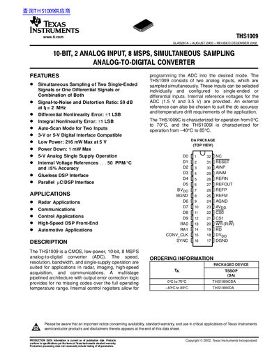
The THS1009 is a CMOS, low-power analog-to-digital converter (ADC) featuring simultaneous sampling of two single-ended signals or one differential signal. It operates at speeds up to 8 MSPS and includes internal voltage references for accurate conversion.
The device supports both parallel microcontroller/DSP interfaces and glueless DSP interfaces. Key features include a multistage pipelined architecture with output error correction logic, ensuring no missing codes over the full operating temperature range.
| Resolution | 10 Bits |
|---|---|
| Sampling Rate | 8 MSPS |
| Signal-to-Noise and Distortion Ratio (Differential) | 59 dB at f = 2 MHz |
| Integral Nonlinearity Error | +1 LSB |
| Differential Nonlinearity Error | +1 LSB |
| Max Power Dissipation | 216 mW at 5 V |
The THS1009C is characterized for operation from 0°C to 70°C, and the THS1009I is characterized for operation from -40°C to 85°C.
Yes, it can simultaneously sample two single-ended signals or one differential signal.