
stlc1511 is a new wide dynamic range analog front end chip from st. it uses a 14-bit nyquist rate da converter and a programmable gain amplifier. it supports 0~-32db transmit gain and 0~40db receive gain. it integrates a phase-locked loop with an external LC or crystal oscillator. the power consumption is only 300mw.
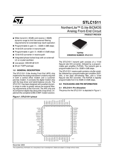
The STLC1511 is a G.lite BICMOS Analog Front-End (AFE) circuit designed for use in both central office and customer premise modems. It connects a digital modem chip with loop driver and hybrid balance circuits to implement a complete G.992.2 DMT modem solution. The device is available in a 64-pin TQFP package.
| Transmit Dynamic Range | ~80dB |
|---|---|
| Receive Dynamic Range | ~69dB |
| Transmit Gain Range | 0 to -32dB |
| Transmit D/A Converter | 14-bit |
| Receive Gain Range | 0 to 40dB |
| Receive A/D Converter | 12-bit |
| Operating Voltage | 5.0V |
| Package Type | 64-pin TQFP |
The transmit gain is programmable from 0 to -32dB in 2dB steps.
The receive gain is programmable from 0 to 40dB in 0.5dB steps.