
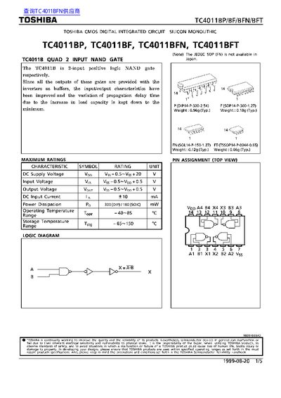
This document provides technical specifications for the Toshiba TC4011BP/BF/BFN/BFT family of CMOS digital integrated circuits. It describes the device as a Quad 2-Input NAND Gate with improved input/output characteristics due to buffer inverters.
The datasheet details maximum ratings, recommended operating conditions, static and dynamic electrical characteristics across various supply voltages (3V to 18V), and includes outline drawings for DIP, SOP, SOIC, and TSSOP packages.
| Product Type | Quad 2-Input NAND Gate |
|---|---|
| DC Supply Voltage Range | 3 to 18 V |
| Operating Temperature Range | -40~85 C |
| Power Dissipation (DIP) | 300 mW |
| Input Capacitance | 7.5 pF |
A typical DIP14 package weighs 0.969 g.