
This document describes the features and characteristics of the products SN54ALS652, SN54ALS653, SN54AS651, SN54AS652 SN74ALS651A, SN74ALS652A, SN74ALS653, SN74ALS654, SN74AS651, SN74AS652, including independent registers and enables for A and B buses, multiplexed real-time and stored data, choice of true or inverting data paths, choice of 3-state or open-collector outputs to A bus.
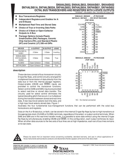
The document describes a family of devices consisting of bus-transceiver circuits, D-type flip-flops, and control circuitry arranged for multiplexed transmission of data directly from the data bus or from internal storage registers. These components feature independent registers and enables for A and B buses, allowing for real-time and stored data transfer without typical decoding glitches.
| Supply Voltage (VCC) | 4.5 V to 5.5 V |
|---|---|
| High-Level Input Voltage (VIH) | 2 V |
| Low-Level Input Voltage (VIL) | 0.8 V |
| High-Level Output Current (IOH) | -15 mA |
| Clock Frequency (fCLOCK) | 0 to 40 MHz |
The SN54ALS family operates over a military temperature range of -55°C to 125°C.
The SN74ALS family operates from 0°C to 70°C.
The -1 versions have an increased recommended maximum output current (Io) of 48 mA compared to standard versions.