
The document contains supplier information for multiple models, including 76007012A, 7600701EA, 7600701FA, 7700401EA, 7700401FA, JM38510/30702B2A, JM38510/30702BEA, JM38510/30702BFA, JM38510/30702SEA, JM38510/30702SFA, SN54LS139AJ, and SN54S139J. These products have different package types, pin counts, package quantities, and environmental plans.
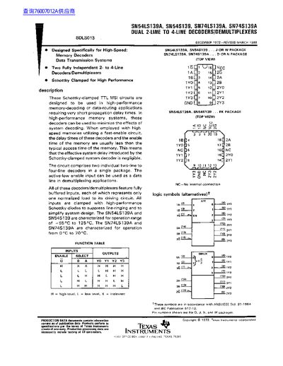
The document describes Schottky-clamped TTL MSI circuits intended for high-performance memory-decoding or data-routing applications. These devices feature two fully independent decoders in a single package with active-low enable inputs that can function as data lines in demultiplexing scenarios.
Key specifications include operation ranges from -55°C to 125°C for the SN54 series and 0°C to 70°C for the SN74 series. The datasheet provides detailed electrical characteristics, switching delays, logic symbols, pin configurations for various packages (D, J, N, W), and a list of available orderable devices with packaging information.
| Supply Voltage (Vcc) | 4.5 V to 5.5 V |
|---|---|
| High-Level Input Voltage (VIH) | 2 V |
| Low-Level Output Current (IOL) | 8 mA |
They are designed to be used in high-performance memory-decoding or data-routing applications requiring very short propagation delay times.
Yes, the active-low enable input can be used as a data line in demultiplexing applications.