
This datasheet introduces the characteristics of the TLC2654 and TLC2654A low-noise chopper-stabilized operational amplifiers
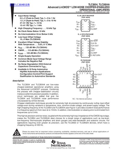
The document describes the TLC2654 and TLC2654A as low-noise, chopper-stabilized operational amplifiers utilizing the Advanced LinCMOS process. These devices are designed for high DC precision with input noise voltage of 0.5 µV peak-to-peak (typical) from 0 to 1 Hz. They feature a high chopping frequency up to 10 kHz and eliminate intermodulation error below 5 kHz, making them suitable for low-level thermocouple amplifiers and strain gauge applications.
| Input Noise Voltage (0 to 1 Hz) | 0.5 µV (Peak-to-Peak) Typ |
|---|---|
| Input Noise Voltage (0 to 10 Hz) | 1.5 µV (Peak-to-Peak) Typ |
| Input Noise Voltage Density (1 kHz) | 13 nV/√Hz Typ |
| Chopping Frequency | 10 kHz Typ |
| Input Offset Voltage (TLC2654A) | 10 µV Max |
| Open-Loop Gain (Min) | 135 dB Min |
| Common-Mode Rejection Ratio (Min) | 110 dB Min |
| Supply Voltage Range | 2.3 V to +8 V |
The typical input noise voltage is 0.5 µV peak-to-peak.
Yes, the typical chopping frequency is 10 kHz.
The maximum input offset voltage for the TLC2654A is 10 µV.
Ranges include 0°C to 70°C, -40°C to 85°C, -40°C to 125°C, and -55°C to 125°C depending on the suffix.