
The Intel® Advanced+ Boot Block Flash Memory (C3) is a feature-rich solution for low-power applications, manufactured on Intel's latest 0.13µm and 0.18µm technologies. The C3 device incorporates low-voltage capability (3V read, program, and erase) with high-speed, low-power operation. Flexible block locking allows any block to be independently locked or unlocked. The Intel® Flash Data Integrator (FDI) software provides a cost-effective, flexible, monolithic code plus data storage solution.
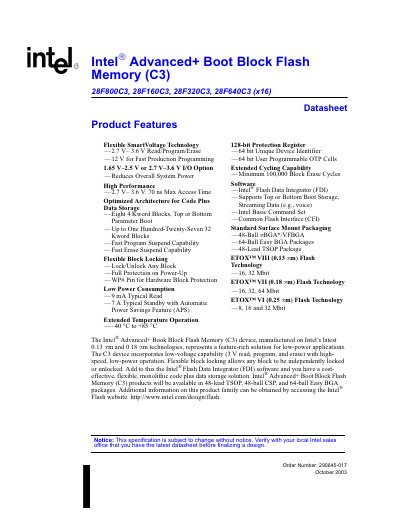
The Advanced+ Boot Block Flash Memory (C3) family offers low‑voltage (3 V) read, program and erase operation with high‑speed, low‑power performance. Devices are available in 48‑lead TSOP, 48‑ball CSP, and 64‑ball Easy BGA packages, supporting both 1.65 V–2.5 V and 2.7 V–3.6 V I/O voltage options.
Key features include flexible block locking, a 128‑bit protection register, 64‑bit unique device identifier, 64‑bit user‑programmable OTP cells, and automatic power‑saving modes (APS, standby, deep power‑down). The datasheet also details thermal limits, DC/AC characteristics, and mechanical dimensions for each package type.
| Read/Program/Erase Voltage | 3 V |
|---|---|
| I/O Voltage Options | 1.65 V–2.5 V or 2.7 V–3.6 V |
| Typical Read Current | 9 mA |
| Typical Standby Current | 7 µA |
| Operating Temperature Range | -40 °C to +85 °C |
| Protection Register Size | 128 bits |
| Unique Device Identifier | 64 bits |
| User Programmable OTP Cells | 64 bits |
| Minimum Block Erase Cycles | 100,000 |
| Package Options | 48‑lead TSOP, 48‑ball CSP, 64‑ball Easy BGA |
The device supports either 1.65 V–2.5 V or 2.7 V–3.6 V I/O voltage options.
The flash memory is rated for a minimum of 100,000 block erase cycles.
The device includes Automatic Power Savings (APS), standby mode, and deep power‑down mode.
They are offered in 48‑lead TSOP, 48‑ball VF BGA, 48‑ball µBGA, and Easy BGA packages.