
M66850J/FP,M66851J/FP,M66852J/FP,M66853J/FP are high-speed synchronous FIFO(First-In,First-Out) memories fabricated by high-speed CMOS technology. These FIFOs are applicable for a data buffer as networks and communications.
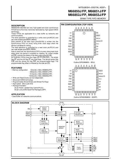
The Mitsubishi M66850J/FP, M66851J/FP, M66852J/FP and M66853J/FP are high‑speed, clock‑synchronous SRAM FIFO memories built with advanced CMOS technology. They provide configurable depths from 64 to 1024 words of 9‑bit data and are intended for use as data buffers in network and communication applications.
Key features include independent read/write clocks, programmable almost‑empty and almost‑full flags, a 25 ns cycle time, and support for both PLCC and LQFP packages. The datasheet details pin functions, electrical characteristics, timing diagrams, and absolute maximum ratings for designers.
| Memory configuration (M66850J/FP) | 64 words × 9 bits |
|---|---|
| Memory configuration (M66853J/FP) | 1024 words × 9 bits |
| Cycle time | 25 ns |
| Recommended supply voltage | 4.5 V – 5.5 V |
| Data Access Time | 3 ns – 15 ns |
| Output Enable to Output Valid | 3 ns – 13 ns |
| Maximum power dissipation | 450 mW (32‑pin PLCC) / 550 mW (32‑pin LQFP) |
The write operation is controlled by the write clock pin (WCLK) and two write‑enable pins (WEN1, WEN2).
When the RS pin is driven low, internal read and write pointers are set to the first location, the output register is cleared, and the flags are initialized.