
MCM67J618B is a 1,179,648 bit synchronous static random access memory designed to provide a burstable, high–performance, secondary cache for the i486 and Pentium microprocessors.
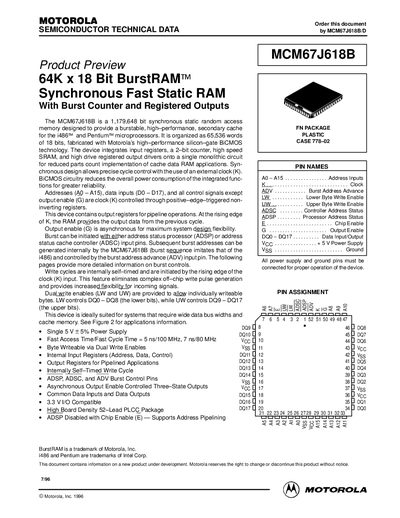
The MCM67J618B is a 1,179,648‑bit synchronous static RAM designed as a high‑performance secondary cache for i486 and Pentium microprocessors. It is organized as 64K × 18 bits and fabricated with Motorola’s high‑performance silicon‑gate BICMOS technology, integrating input registers, a 2‑bit counter, and registered output drivers.
Key features include burst operation initiated by ADSP or ADSC pins, dual‑byte write enables, asynchronous output enable, and operation from a single 5 V supply. The device is offered in a 52‑lead PLCC package and meets the specified DC and AC timing and electrical characteristics for reliable high‑speed memory applications.
| Memory Organization | 64K × 18 bits (1,179,648 bits) |
|---|---|
| Supply Voltage (Vcc) | 4.75 V – 5.25 V |
| Access Time / Cycle Time | 5 ns @100 MHz, 7 ns @80 MHz |
| Input Capacitance | 4 – 5 pF |
| Output Low Voltage (VOL) | 0.4 V |
| Package | 52‑lead PLCC |
Burst can be started with either the ADSP (address status processor) or ADSC (address status cache controller) input pins, and subsequent burst addresses are generated internally.
The device operates from a 5 V supply with a recommended range of 4.75 V to 5.25 V.
The chip is supplied in a 52‑lead PLCC package (case 778‑02).