
The MCM64PC32 (256K) and MCM64PC64 (512K) are designed to provide a burstable, high performance, L2 cache for the Pentium microprocessor in conjunction with Intel’s Triton II chip set. The MCM64PC32 is configured as 32K x 64 bits and the MCM64PC64 is configured as 64K x 64 bits. Both are packaged in a 160 pin card edge memory module. Each module uses Motorola’s 3.3 V 32K x 32 BurstRAMs and one Motorola 3.3 V 32K x 8 FSRAM for the tag RAM. Bursts can be initiated with either address status processor (ADSP) or cache address status (CADS). Subsequent burst addresses are generated internal to the BurstRAM by the cache burst advance (CADV) input pin. Write cycles are internally self timed and are initiated by the rising edge of the clock (CLK0) input. Eight write enables are provided for byte write control. PD0-PD3 map into the Triton II chip set for auto-configuration of the cache control. Pentium-Style Burst Counter on Chip. Pipelined Data Out. 160 Pin Card Edge Module. Address Pipeline Supported by ADSP Disabled with Ex. All Cache Data and Tag I/Os are TTL Compatible. Three State Outputs. Byte Write Capability. Fast Module Clock Rate: 66 MHz. Fast SRAM Access Times: 15 ns for Tag RAM, 8 ns for Data RAMs. One-Cycle Deselect Data RAMs. Decoupling Capacitors for Each Fast Static RAM. High Quality Multi-Layer FR4 PWB with Separate Power and Ground.
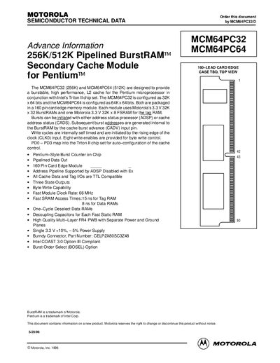
This Motorola datasheet describes the MCM64PC32 (256 K) and MCM64PC64 (512 K) secondary cache modules designed for Pentium microprocessors. It includes block diagrams, pin assignments, truth tables, and electrical characteristics for both the 32‑bit and 64‑bit configurations.
The document provides absolute maximum ratings, recommended operating conditions, AC and DC performance data, package dimensions, and contact information for Motorola literature distribution.
| Cache Size | 256 K (MCM64PC32) / 512 K (MCM64PC64) |
|---|---|
| Module Clock Rate | 66 MHz |
| SRAM Access Times | 15 ns (Tag RAM), 8 ns (Data RAMs) |
| Supply Voltage (Operating Range) | 3.135 V – 3.6 V |
| Power Supply Voltage (Absolute Max) | -0.5 V to +46 V |
| Operating Temperature Range | 20 °C – 110 °C |
| Package Thickness (160‑lead card edge) | 0.285 in – 0.305 in |
The MCM64PC32 provides a 256 K cache, configured as 32 K × 64 bits.
The recommended operating supply voltage is 3.135 V to 3.6 V (Vpp).
BOSEL is the Burst Order Select pin; it is NC for an interleaved burst counter and should be tied to ground for a linear burst counter.
The device operates from 20 °C up to 110 °C.