
This document is about MC74HC367A technical data sheet. The chip has a 15 LSTTL load drive capability, outputs directly interface to CMOS, NMOS, TTL, operating voltage range is 2 to 6V, input current is 1µA, complies with JEDEC standard 7A requirements, and chip complexity is 92 FETs or 23 equivalent gates.
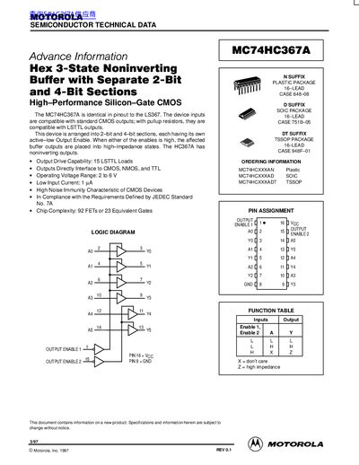
The MC74HC367A is a 3‑state non‑inverting buffer with separate 2‑bit and 4‑bit sections, each having its own active‑low output enable. It is pin‑compatible with the LS367 and compatible with standard CMOS, LSTTL, and TTL outputs.
The document lists maximum ratings, recommended operating conditions, DC and AC electrical characteristics, propagation delays, and detailed outline dimensions for plastic DIP, SOIC, and TSSOP packages. It also includes test circuits, switching waveforms, and mechanical drawing data.
| Operating Voltage Range | 2 to 6 V |
|---|---|
| Output Drive Capability | 15 LSTTL loads |
| Power Dissipation (Plastic DIP) | 750 mW |
| Input Current per Pin | 20 mA |
| Output Current per Pin | 25 mA |
| Maximum Input Capacitance | 10 pF |
| Package Options | Plastic DIP, SOIC, TSSOP |
The device operates from 2 V to 6 V.
Each output pin can source up to 25 mA.
The DIP package can dissipate up to 750 mW in still air.
The part is offered in Plastic DIP, SOIC, and TSSOP packages.