
The CLC5612 is a dual, low-cost, high-speed (90MHz) buffer which features user-programmable gains of +2, +1, and -1V/V. It offers 0.1dB gain flatness to 18MHz and differential gain and phase errors of 0.15% and 0.02°. These features are ideal for professional and consumer video applications.
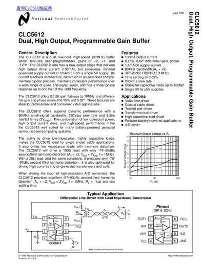
The CLC5612 is a dual, low‑cost, high‑speed buffer that offers user‑programmable gains of +2, +1, and –1 V/V. It delivers a high output drive current (130 mA) while consuming minimal quiescent supply current (1.5 mA per channel) from a single 5 V supply.
The device features a 90 MHz –3 dB bandwidth at a gain of +2, a 290 V/µs slew rate, and can drive low‑impedance, highly capacitive loads with low distortion, making it suitable for video line drivers, A/D driver applications, and portable battery‑powered systems.
| Programmable gains | +2, +1, -1 V/V |
|---|---|
| Maximum output current | 130 mA |
| Supply current per channel | 1.5 mA |
| Slew rate | 290 V/µs |
It operates from a single 5 V supply or dual +5 V supplies.
The CLC5612 can source up to 130 mA of output current.