
The CLC5665 is a low-cost, wideband amplifier that provides very low 2nd and 3rd harmonic distortion at 1MHz (-89/-92dBc). The great slew rate of 1800V/µs, bandwidth of 90MHz (Av = +1) and fast disable make it an excellent choice for many high speed multiplexing applications. Like all current feedback op amps, the CLC5665 allows the frequency response to be optimized (or adjusted) by the selection of the feedback resistor. For demanding video applications, the 0.1dB bandwidth to 20MHz and differential gain/phase of 0.05%/0.05° make the CLC5665 the preferred component for broadcast quality NTSC and PAL video systems. The large voltage swing (28Vpp), continuous output current (85mA) and slew rate (1800V/µs) provide high-fidelity signal transmission.
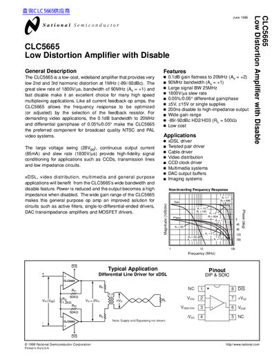
The CLC5665 is a low‑cost, wideband current‑feedback amplifier offering 0.1 dB gain flatness to 20 MHz, high slew rate, and a fast enable/disable function. It is suited for video, xDSL, multimedia, and general‑purpose applications where low distortion and wide bandwidth are required.
The document provides electrical characteristics, design considerations, and example circuits such as level‑shifting, multiplexing, differential line drivers, and CCD clock drivers. It also includes ordering information, reliability notes, and a life‑support policy for the component.
| Slew rate | 1800 V/µs |
|---|
The device enables when the pin‑8 voltage is above 12.7 V (for a +15 V supply) or above 2.7 V (for a +5 V supply), and disables when the voltage is below 10.0 V or below 0.8 V respectively.