
The DS16149-DS36149 and DS16179-DS36179 are Hex MOS drivers with outputs designed to drive large capacitive loads up to 500 pF associated with MOS memory systems. PNP input transistors are employed to reduce input currents allowing the large fan-out to these drivers needed in memory systems. The circuit has Schottky-clamped transistor logic for minimum propagation delay and a disable control that places the outputs in the logic ‘‘1’’ state. This is especially useful in MOS RAM applications where a set of address lines has to be in the logic ‘’1’’ state during refresh. The DS16149-DS36149 has a 15 X resistor in series with the outputs to dampen transients caused by the fast-switching output. The DS16179-DS36179 has a direct low impedance output for use with or without an external resistor.
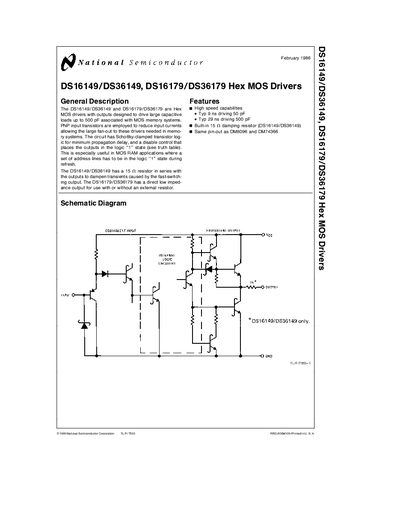
The DS16149/DS36149 and DS16179/DS36179 are hex MOS drivers designed for large capacitive loads up to 500 pF in MOS memory systems. They feature Schottky‑clamped transistors for low propagation delay and a disable control that forces outputs to a logic “1” state.
The document provides absolute maximum ratings, operating conditions, DC electrical characteristics, switching performance, physical dimensions, and a life‑support policy notice. It also lists typical applications and package information for both ceramic and molded dual‑inline packages.
| Typical propagation delay (50 pF) | 9 ns |
|---|---|
| Typical propagation delay (500 pF) | 29 ns |
| Maximum power dissipation (cavity package) | 1371 mW |
| Maximum power dissipation (molded package) | 1280 mW |
| Supply voltage range | 4.5 V – 5.5 V |
The maximum supply voltage is 5.5 V.
The typical propagation delay is 29 ns.
The ceramic package can dissipate up to 1371 mW, and the molded package up to 1280 mW.
No, National Semiconductor does not authorize their use as critical components in life‑support devices without written approval.