
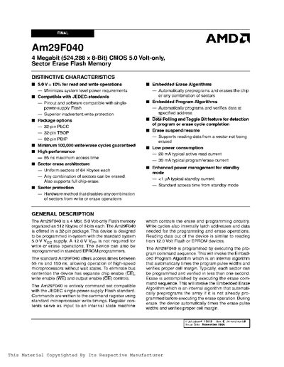
The Am29F040 is a 4 Mbit (524,288 × 8‑bit) CMOS flash memory that operates from a single 5.0 V supply. It offers sector‑erase architecture with 64 KB uniform sectors, low power consumption, and up to 100,000 guaranteed write/erase cycles.
The datasheet provides detailed electrical characteristics, timing diagrams, pin configurations for PDIP, PLCC, and TSOP packages, and command sequences for programming, erasing, and sector protection.
| Memory size | 4 Mbit (524,288 × 8 bits) |
|---|---|
| Operating voltage | 5.0 V ±10 % |
| Maximum access time | 55 ns |
| Typical active read current | 20 mA |
| Typical program/erase current | 30 mA |
| Standby current (typical) | < 1 nA |
| Write/erase cycle endurance | ≥ 100,000 cycles |
| Sector size | 64 KB |
| Package options | 32‑pin PLCC, 32‑pin TSOP, 32‑pin PDIP |
The device operates from a single 5.0 V supply (±10 %).
The datasheet guarantees a minimum of 100,000 write/erase cycles.
The maximum access time is specified as 55 ns.
Each sector is 64 KB in size.