
CY7C1381C/CY7C1383C is a 3.3V synchronous flow-through SRAM designed to interface with high-speed microprocessors with minimum glue logic. It features support for 133-MHz bus operations, 512K x 36 and 1M x 18 common I/O, high-performance access rate, and more.
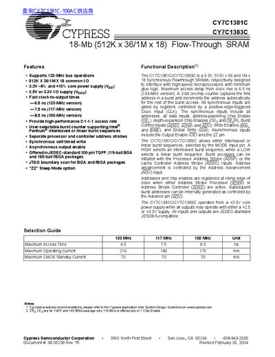
The CY7C1381C (512K × 36) and CY7C1383C (1M × 18) are synchronous flow‑through SRAMs designed for high‑speed microprocessor interfaces. They support bus speeds up to 133 MHz, provide fast clock‑to‑output times (6.5 ns at 133 MHz) and feature selectable burst modes via the MODE pin.
The devices are supplied in JEDEC‑standard 100‑pin TQFP, 119‑ball BGA and 165‑ball fBGA packages and operate from a 3.3 V core supply with either 2.5 V or 3.3 V I/O supplies. Detailed pin definitions, timing tables and package diagrams are included in the document.
| Memory capacity | 512K × 36 (CY7C1381C) / 1M × 18 (CY7C1383C) |
|---|---|
| Maximum access time | 6.5 ns (133 MHz version) |
| Maximum operating current | 210 mA (133 MHz version) |
| Maximum CMOS standby current | 70 mA |
| Supported bus speed | Up to 133 MHz |
| Core power supply | 3.3 V |
| I/O power supply | 2.5 V or 3.3 V |
| Package options | 100‑pin TQFP, 119‑ball BGA, 165‑ball fBGA |
They support bus operations up to 133 MHz.
The core runs from a 3.3 V supply, and the I/O pins can be powered at either 2.5 V or 3.3 V.
They are offered in 100‑pin TQFP, 119‑ball BGA and 165‑ball fBGA packages.