
The CY2SSTV8575 is a high-performance, low-skew, low jitter zero-delay buffer designed to distribute differential clocks in high-speed applications. It generates five differential pair clock outputs from one differential pair clock input, and features differential feedback clock outputs and inputs. It supports an operating frequency of 60 MHz to 170 MHz, and is compatible with 266 MHz DDR SDRAM. It has low jitter (cycle-to-cycle) and very low skew, and supports spread spectrum. It also has a power management control input, high-impedance outputs when the input clock is less than 20 MHz, and operates at 2.5V.
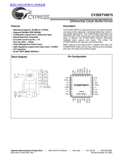
The CY2SSTV8575 is a zero‑delay differential clock buffer that generates five differential pair outputs from a single differential input. It features low jitter (< 75 ps) and very low skew (< 100 ps), making it suitable for high‑speed clock distribution and nested clock‑tree applications. The device includes a PLL that can be bypassed for test purposes and supports power‑management via an output‑enable control.
The datasheet provides detailed electrical specifications, including operating frequency (60 MHz‑170 MHz), supply voltage (2.5 V nominal), input frequency range, jitter, skew, propagation delays, and package information (32‑pin TQFP). Ordering information and mechanical drawings are also included.
| Operating frequency | 60 MHz to 170 MHz |
|---|---|
| Low jitter (cycle‑to‑cycle) | < 75 ps |
| Low skew | < 100 ps |
| Supply voltage (VDDQ) | 2.5 V nominal |
| Input frequency range | 60 MHz to 170 MHz |
| Number of differential outputs | 5 |
It operates from 60 MHz up to 170 MHz.
The device provides five differential outputs from a single differential input.
The cycle‑to‑cycle jitter is less than 75 ps.
Power management is done via the output‑enable (OE) pin, which three‑states the outputs when OE is low.