
This document contains information on a product under development at Advanced Micro Devices. The information is intended to help you evaluate this product. AMD reserves the right to change or discontinue work on this proposed product without notice. The product is a Stacked Multi-Chip Package (MCP) consisting of Flash Memory and Static RAM. The Flash Memory has a capacity of 16 Megabits (2 M x 8-Bit/1 M x 16-Bit) and operates at a voltage of 3.0 volts. It features simultaneous read/write operations, secured silicon sector, and zero power operation.
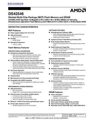
The document provides a detailed description of the Am29DL163D 16‑megabit stacked multi‑chip package (MCP) that combines flash memory and 4 Mbit SRAM. It outlines distinctive characteristics such as simultaneous read/write operation, secured silicon sector, and low‑power modes, and lists the MCP and flash memory features, architectural advantages, and performance characteristics.
Electrical specifications, pin descriptions, device bus operations, command definitions, and test conditions are presented, along with diagrams for the MCP block, flash memory block, and connection layout. The document also includes handling instructions for the 69‑ball FBGA package and information on standby, automatic sleep, and power‑down features.
| Supply Voltage | 2.7 V to 3.3 V |
|---|---|
| Maximum Access Time | 85 ns |
| Active Read Current (1 MHz) | 2 mA |
| Standby Current | 200 nA |
| Write Cycle Endurance | ≥ 1 million cycles per sector |
| Package Type | 69‑Ball FBGA |
The device operates from –25 °C to +85 °C.
Yes, it supports simultaneous read/write with zero latency between the two banks.
Each sector is guaranteed for at least one million write cycles.