
The 54SX family of FPGAs is a leading-edge FPGA with an internal performance of up to 320 MHz, a clock-to-output (pin-to-pin) delay of 3.7 ns, an input setup time of 0.1 ns, and a clock skew of 0.25 ns. The series has 12,000 to 48,000 system gates, up to 249 user-programmable I/O pins, up to 1080 dedicated flip-flops, and is manufactured using a 0.35µ CMOS process. The series also features 66 MHz PCI, CPLD and FPGA integration, a single-chip solution, 100% resource utilization and 100% pin locking, 3.3V operation and 5.0V input tolerance, very low power consumption, deterministic, user-controllable timing, Silicon Explorer II's unique In-System diagnostic and debug capability, boundary scan testing in compliance with IEEE Standard 1149.1 (JTAG), and secure programming technology that prevents reverse engineering and design theft.
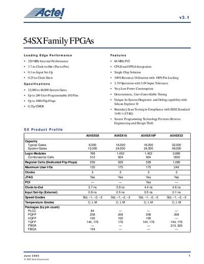
The 54SX family of FPGAs from Actel offers leading‑edge performance with internal clock speeds up to 320 MHz, 3.7 ns clock‑to‑out, and very low power consumption. The architecture uses a sea‑of‑modules design with combinatorial (C‑cell) and register (R‑cell) logic modules, providing deterministic timing and full pin‑locking.
The datasheet lists key specifications such as system gate counts from 12 k to 48 k, up to 249 user‑programmable I/Os, multiple speed grades, and a variety of package options (PLCC, PQFP, TQFP, PBGA, FBGA). Power requirements include 3.3 V operation with 5.0 V input tolerance, and the devices are IEEE 1149.1 compliant for boundary‑scan testing.
| System Gates | 12,000 to 48,000 |
|---|---|
| Maximum User I/Os | 249 |
| Clock‑to‑Out (pin‑to‑pin) | 3.7 ns |
| Input Setup Time | 0.1 ns |
| Clock Skew | 0.25 ns |
| Supply Voltage | 3.3 V operation, 5.0 V input tolerance |
The 54SX devices achieve a clock‑to‑out (pin‑to‑pin) delay of 3.7 ns.
The family operates at 3.3 V and tolerates 5.0 V input levels.
The A54SX32 variant provides up to 249 user‑programmable I/O pins.
Yes, all 54SX devices are IEEE 1149.1 compliant and support boundary‑scan testing.