
The 40MX and 42MX FPGA families are high-capacity, high-performance, highly reliable, and easy-to-integrate products.
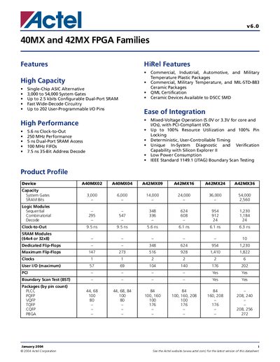
The 40MX and 42MX FPGA families are single‑chip, antifuse‑based devices offering high capacity (3,000‑54,000 system gates) and up to 202 user‑programmable I/Os. They target cost‑effective designs in commercial, industrial, automotive and military temperature ranges and support both 5 V and 3.3 V I/O operation.
The datasheet details electrical specifications (e.g., 5.6 ns clock‑to‑out, 250 MHz performance), power consumption, package options (plastic and ceramic PLCC, PQFP, VQFP, BGA), timing models, and PCI compliance. It also includes ordering information, temperature grades, and recommended operating conditions.
| User‑Programmable I/O Pins | Up to 202 |
|---|---|
| Clock‑to‑Out Time | 5.6 ns |
| Maximum Performance Frequency | 250 MHz |
| Commercial Temperature Range | 0 to +70 °C |
| Industrial Temperature Range | –40 to +85 °C |
The devices provide up to 202 user‑programmable I/O pins.
The clock‑to‑out delay is 5.6 ns.
Commercial‑grade devices operate from 0 °C to +70 °C.
They can operate up to 250 MHz.