
The 54SX family of FPGAs is a high-performance FPGA chip from Actel Corporation, using a 0.35-micron CMOS process, with 320MHz internal performance, 3.7ns pin-to-pin clock-to-output delay, 0.1ns input setup time, and 0.25ns clock jitter. It can support up to 12,000 to 48,000 system gates, 249 user-programmable I/O pins, and 1080 dedicated flip-flops.
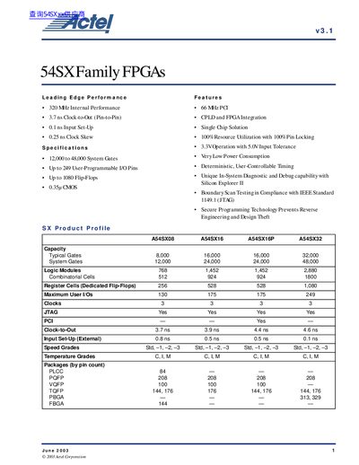
The Actel 54SX family of FPGAs delivers high‑speed internal performance up to 320 MHz with a 3.7 ns clock‑to‑out time and very low power consumption. The devices feature a sea‑of‑modules architecture, offering 12 000 to 48 000 system gates, up to 249 user‑programmable I/O pins, and deterministic timing with built‑in diagnostics.
The family supports 3.3 V operation with 5.0 V input tolerance, multiple package options (PLCC, PQFP, VQFP, TQFP, PBGA, FBGA), and full IEEE 1149.1 boundary‑scan compliance. Development tools include Actel DeskTOP and Designer Advantage, plus built‑in ActionProbe circuitry for real‑time logic analysis.
| Internal Performance | 320 MHz |
|---|---|
| Clock‑to‑Out (Pin‑to‑Pin) | 3.7 ns |
| System Gates | 12 000 – 48 000 |
| User‑Programmable I/O Pins | Up to 249 |
| Supply Voltage | 3.3 V operation, 5.0 V input tolerance |
| Package Options | PLCC 84, PQFP 208, VQFP 100, TQFP 144/176, PBGA 313/329, FBGA 144 |
The devices achieve a clock‑to‑out time of 3.7 ns.
The A54SX32 device provides approximately 48 000 system gates.
The family operates at 3.3 V and tolerates 5.0 V input levels.
Yes, all SX devices are IEEE 1149.1 (JTAG) compliant.