
This document introduces a 32 Mbit flash memory chip called M59DR032A and M59DR032B, which features low voltage supply, fast programming and erasing, dual bank memory array, block protection/unlocking, etc.
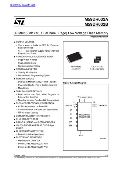
This handbook describes the 32 Mbit (2 Mb × 16) low‑voltage flash memory devices M59DR032A and M59DR032B. It includes preliminary data, electrical characteristics, package information, and detailed command sequences for programming, erasing, and reading the memory.
The document also covers dual‑bank operation, block protection, automatic standby, power‑down modes, and the Common Flash Interface (CFI) query. Pin‑out diagrams for TSOP48 and FBGA48 packages are provided along with memory organization tables and timing specifications.
| Programming Supply Voltage (Vppa) | 1.65 V to 2.2 V |
|---|---|
| Optional Fast Program Voltage (Vpp) | 12 V |
| Page Access Time | 35 ns |
| Random Access Time | 100 ns |
| Typical Programming Time per Word | 10 µs |
| Data Retention | 20 years |
| Program/Erase Cycle Endurance | 100,000 cycles |
| Operating Temperature Range | -40 °C to 85 °C |
| Storage Temperature Range | -55 °C to 155 °C |
| Package Types | TSOP48 (12 × 20 mm) and FBGA48 (0.75 mm ball pitch) |
The device is rated for 100,000 program/erase cycles.
Data is retained for 20 years.
The memory operates from –40 °C to 85 °C.