
The C8051F040/1/2/3/4/5/6/7 is a mixed signal ISP flash MCU produced by Silicon Laboratories. Its features include a 10 or 12-bit SAR ADC, an 8-bit SAR ADC, two 12-bit DACs, three analog comparators, a voltage reference, a precise VDD monitor/brownout detector, on-chip JTAG debug and boundary scan, and a high-speed 8051µC core with pipelined instruction architecture.
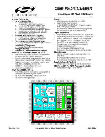
This manual describes the C8051F040 family of mixed‑signal 8051‑compatible microcontrollers. It covers the high‑speed core, on‑chip memory options, analog peripherals such as SAR ADCs, DACs, comparators, and a built‑in temperature sensor, as well as digital interfaces like CAN, SMBus, SPI, and UART.
The document includes sections on system architecture, clock sources, power‑management modes, pinout and package definitions, and detailed register descriptions for peripherals. It also provides programming guidance for flash memory, XRAM, and peripheral configuration, plus a change list and contact information for Silicon Labs.
| Supply Voltage | 2.7 to 3.6 V |
|---|---|
| Operating Temperature Range | ‑40 to +85 °C |
| Package Options | 100‑Pin and 64‑Pin TQFP |
| Internal Oscillator Range | 3 to 24.5 MHz |
| Maximum CPU Throughput | Up to 25 MIPS (25 MHz clock) |
| Internal RAM | 4352 bytes (4 k + 256 B) |
| Flash Memory Size | 64 kB (C8051F040/1/2/3/4/5) or 32 kB (C8051F046/7) |
| ADC Resolution | 12‑bit (C8051F040/1) or 10‑bit (C8051F042/3/4/5/6/7) |
| Interrupt Sources | 20 vectored interrupt sources |
The device operates from 2.7 V to 3.6 V.
It provides 20 vectored interrupt sources.
Both 100‑Pin and 64‑Pin TQFP packages are offered.
The core can reach up to 25 MIPS when run at a 25 MHz clock.