
This document is about the AD768 datasheet. AD768 is a 16-bit high-precision ADC manufactured by ADI. It supports 30MSPS conversion rate and has good dynamic range and low distortion characteristics.
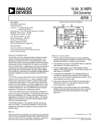
The AD768 is a high‑speed 16‑bit digital‑to‑analog converter that uses a segmented current‑source architecture combined with an R‑2R ladder for the lower bits. It features edge‑triggered input latches, an on‑chip temperature‑compensated 2.5 V bandgap reference, and can be powered from ±5 V supplies.
Key specifications include a typical power dissipation of 465 mW, a full‑scale output current of 20 mA into a 1 kΩ load, an update rate up to 40 MSPS, and an operating temperature range of –40 °C to +85 °C. The device is offered in a 28‑pin SOIC package and is suited for applications such as arbitrary waveform generation, communications, and waveform reconstruction.
| Resolution | 16 Bits |
|---|---|
| Maximum Output Update Rate | 30‑40 MSPS |
| Full‑Scale Output Current | 20 mA (nominal) |
| Output Impedance | 1 kΩ |
| Power Dissipation (typical) | 465 mW |
| Supply Voltage | ±5 V |
| Operating Temperature Range | –40 °C to +85 °C |
The AD768 provides a nominal full‑scale output current of 20 mA.
The device can update up to 40 MSPS, with a typical rate of 30 MSPS.
It operates from ±5 V supplies.
The output impedance is 1 kΩ.