
This is the functional block diagram of AD8582. It is a complete dual 12-bit DAC with no external components, single +5V operation, 1 mV/Bit with 4.095 V full scale, true voltage output, ±5 mA drive, and very low power consumption: 5 mW.
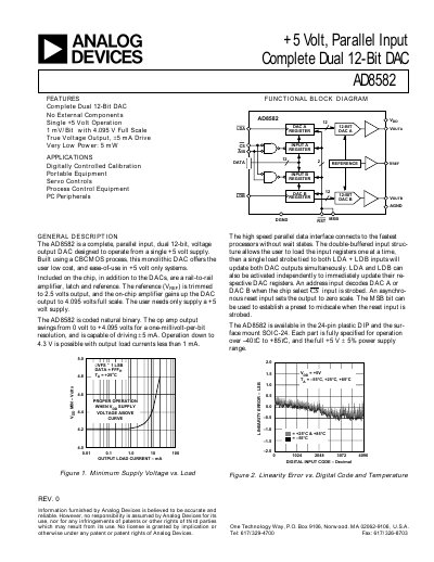
The AD8582 is a complete, parallel‑input, dual 12‑bit voltage‑output DAC designed for single‑supply (+5 V) operation. It integrates a rail‑to‑rail reference, low‑power amplifier and dual DAC cores, providing 1 mV/LSB resolution and up to ±5 mA output drive.
The device is offered in 24‑pin DIP and 24‑lead SOIC packages, operates from –40 °C to +85 °C, and includes features such as double‑buffered input registers, independent load strobes (LDA/LDB), and ESD protection. Detailed electrical, timing, and performance specifications are provided in the datasheet.
| Supply Voltage | +5.0 V ± 5% |
|---|---|
| Logic Low Input Voltage (VIL) | 0.8 V |
| Logic High Input Voltage (VIH) | 2.4 V |
| Operating Temperature Range | –40 °C to +85 °C |
| Package Options | 24‑pin DIP and 24‑lead SOIC |
It operates from a single +5 V supply with a tolerance of ±5 %.
Logic low is recognized at 0.8 V (VIL) and logic high at 2.4 V (VIH).