
This document introduces the function characteristics of ADV7121/ADV7122, including 80MHz sampling rate, triple 10-bit D/A converters, RS-343A/RS-170 compatible outputs, TTL compatible inputs, +5V CMOS monolithic construction, 40-pin DIP package (ADV7121), 44-pin PLCC package (ADV7122) and 48-lead TQFP (ADV7122)
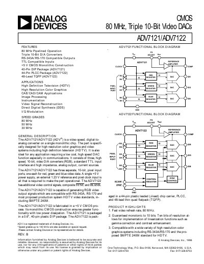
This document describes the ADV7121 and ADV7122 video digital‑to‑analog converters, three 10‑bit DACs designed for high‑resolution color graphics, HDTV and other video applications. It includes functional block diagrams, pin configurations, and detailed electrical characteristics.
Key sections cover static and dynamic performance specifications, timing characteristics, absolute maximum ratings, pin descriptions, and recommended reference circuitry. The datasheet also lists ordering information for the 40‑pin DIP, 44‑pin PLCC and 48‑lead TQFP packages.
| Resolution | 10 Bits |
|---|---|
| Integral Nonlinearity (INL) | ±2 LSB max |
| Differential Nonlinearity (DNL) | ±1 LSB max |
| Gray Scale Error | ±5 % |
| Gray Scale Current Range | 15 mA min – 22 mA max |
| Supply Voltage (VAA) | 5 V |
| Power Dissipation (max) | 625 mW |
| Package Options | 40‑Pin DIP (ADV7121), 44‑Pin PLCC (ADV7122), 48‑Lead TQFP (ADV7122) |
An external 1.23 V voltage reference must be connected to the VREF pin.
The ambient operating temperature is 0 °C to +70 °C; storage temperature is –65 °C to +150 °C.
The BLANK pin provides composite blank control and the SYNC pin provides composite sync control; both are TTL compatible.