
The DAC8412/DAC8413 are quad, 12-bit voltage output DACs with readback capability. Built using a complementary BiCMOS process, these monolithic DACs offer the user very high package density. Output voltage swing is set by the two reference inputs VREFH and VREFL. By setting the VREFL input to 0 V and VREFH to a positive voltage, the DAC provides a unipolar positive output range. A similar configuration with VREFH at 0 V and VREFL at a negative voltage provides a unipolar negative output range. Bipolar outputs are configured by connecting both VREFH and VREFL to nonzero voltages. This method of setting output voltage range has advantages over other bipolar offsetting methods because it is not dependent on internal and external resistors with different temperature coefficients. Digital controls allow the user to load or read data.
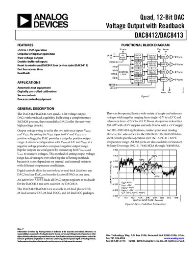
The DAC8412 and DAC8413 are quad, 12‑bit voltage‑output digital‑to‑analog converters with readback capability. They operate from +5 V to +15 V supplies and support both unipolar and bipolar output configurations using separate reference inputs.
The document provides detailed electrical characteristics, absolute maximum ratings, thermal resistance data, pin descriptions, typical performance curves, and an ordering guide for the various 28‑lead package options (PDIP, CERDIP, PLCC, LCC).
| Supply Voltage Range | +5 V to +15 V |
|---|---|
| Power Dissipation (15 V supply) | 330 mW |
| Power Dissipation (5 V supply) | 60 mW |
| Integral Nonlinearity (INL) – E grade | +0.25 LSB |
| Differential Nonlinearity (DNL) | -1 LSB (monotonic over temperature) |
| Slew Rate | 2.2 V/µs |
An active‑low reset loads all DAC output registers to midscale for the DAC8412.
The devices are offered in 28‑lead plastic DIP, 28‑lead ceramic DIP, 28‑lead PLCC, and 28‑lead LCC packages.
The MIL‑STD‑883 versions operate from –55 °C to +125 °C.
Typical power dissipation is about 60 mW when powered from a +5 V supply.