
This data sheet is applicable to CD54/74AC299, CD74AC323, CD54/74ACT299, and CD54ACT323. The CD54AC323 and CD74ACT323 were not acquired from Harris Semiconductor. Data sheet acquired from Harris Semiconductor SCHS288.
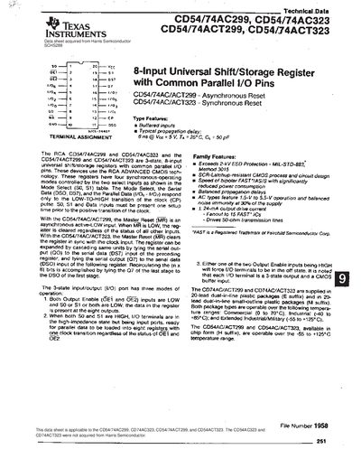
The CD54/74AC299 (and related CD54/74AC323, CD54/74ACT299, CD54/74ACT323) are 8‑input universal shift/storage registers with common parallel I/O pins. They feature buffered inputs, three‑state I/O, and four synchronous operating modes controlled by two select inputs. The devices use RCA Advanced CMOS technology and support both asynchronous and synchronous master reset functions.
Key specifications include a typical propagation delay of 6 ns, 24 mA output drive current, a supply voltage range of 0.5 V to 6 V, and an operating temperature range of –55 °C to +125 °C. The parts are offered in 20‑lead dual‑in‑line (E) and small‑outline (M) plastic packages, with power dissipation up to 500 mW depending on temperature.
| Output drive current | 24 mA |
|---|
The master reset (MA) is an asynchronous active‑LOW input; when MA is LOW the register is cleared regardless of the status of all other inputs.