
This document describes the features and characteristics of the C8051F2xx MCU family, including SAR ADC with 12-bit and 8-bit resolution, two comparators, VDD monitor and brown-out detector, On-Chip JTAG debug, high-speed 8051 mC core, memory, and digital peripherals.
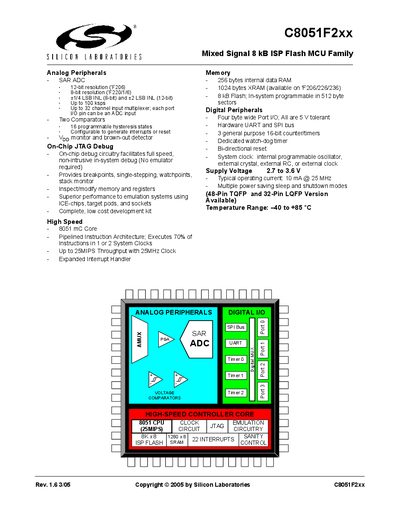
The C8051F2xx family is a mixed‑signal 8 kB ISP flash microcontroller series featuring a high‑speed 8051 core, up to 25 MIPS at 25 MHz, 256 bytes internal RAM, 1 KB XRAM, and a range of analog peripherals such as 8‑bit and 12‑bit SAR ADCs, two programmable comparators, and a voltage‑monitor/brown‑out detector. The devices operate from 2.7 V to 3.6 V and support multiple power‑saving modes.
The manual covers system overview, pinout and package definitions, detailed descriptions of the CPU core, memory organization, JTAG debug, digital I/O, serial interfaces (UART, SPI), timer modules, ADC operation, comparator characteristics, voltage reference, power‑management modes, flash programming commands, reset sources, oscillator options, and contact information for Silicon Labs.
| Flash Memory Size | 8 kB ISP Flash |
|---|---|
| Internal Data RAM | 256 bytes |
| External XRAM (available on selected parts) | 1 KB |
| Maximum Clock Frequency | 25 MHz |
| Maximum MIPS | 25 MIPS |
| Supply Voltage Range | 2.7 V to 3.6 V |
| Typical Operating Current @ 25 MHz | 10 mA |
| Operating Temperature Range | -40 °C to +85 °C |
| ADC Resolution (8‑bit part) | 8‑bit |
| ADC Resolution (12‑bit part) | 12‑bit |
| Maximum ADC Sample Rate | 100 ksps |
| Number of ADC Channels | Up to 32 |
The C8051F2xx operates from 2.7 V to 3.6 V.
It can deliver up to 25 MIPS at a 25 MHz clock.
Typical operating current is about 10 mA.
The MCU provides 256 bytes of internal data RAM.