
DS26C31T/DS26C31M CMOS Quad TRI-STATE® Differential Line Driver is a quad differential line driver designed for digital data transmission over balanced lines, which meets all the requirements of EIA standard RS-422, while retaining the low power characteristics of CMOS.
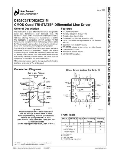
The DS26C31T and DS26C31M are quad differential line drivers designed for RS‑422 balanced data transmission. They accept TTL or CMOS inputs and provide low‑power, tri‑state outputs that can be disabled without loading the bus. The devices are pin‑compatible with the AM26LS31 and DS26LS31 and include ESD protection on all inputs.
The document provides absolute maximum ratings, DC and switching electrical characteristics, typical performance graphs, and mechanical dimensions for several surface‑mount packages (M, W, E, N). It also contains application notes, a life‑support policy, and customer support information.
| Supply Voltage (Vcc) | -0.5 V to 7.0 V |
|---|---|
| Typical Propagation Delay | 6 ns |
| Typical Output Skew | 0.5 ns |
| Input High Level Voltage (Vin) | 2.0 V |
| Input Low Level Voltage (Vit) | 0.8 V |
| Maximum Output Current per Pin | 150 mA |
| Package Options | M, N, W, E (surface‑mount) |
The device operates from –0.5 V to 7.0 V supply voltage.
Typical propagation delay is 6 ns and typical output skew is 0.5 ns.
The DS26C31 is offered in several surface‑mount packages, including M (dual‑in‑line), N (dual‑in‑line), W (ceramic flat‑pack) and E (ceramic leadless chip carrier).
Each output pin can source up to 150 mA.