
The MC14001B series is a CMOS gate circuit constructed with P and N channel enhancement mode devices. Its primary use is in applications where low power dissipation and/or high noise immunity is desired. The supply voltage range is 3.0 Vdc to 18 Vdc, and all outputs are buffered. It is capable of driving two low-power TTL loads or one low-power Schottky TTL load over the rated temperature range. The inputs have double diode protection, except for MC14011B and MC14081B which have triple diode protection.
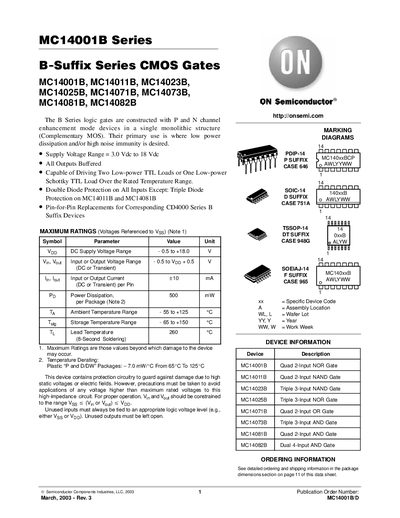
The MC14001B Series comprises B‑suffix CMOS logic gates built with complementary MOS devices for low power dissipation and high noise immunity. The series includes quad 2‑input NOR, NAND, OR, AND gates, as well as triple 3‑input NAND/NOR and dual 4‑input AND gates.
The data sheet details supply voltage ranges, maximum ratings, switching times, typical voltage transfer characteristics, package dimensions for PDIP‑14, SOIC‑14 and TSSOP‑14, and ordering/shipping information for each device variant.
| Supply Voltage Range | 3.0 Vdc to 18 Vdc |
|---|---|
| Power Dissipation per Package | 500 mW |
| Ambient Temperature Range | -55 °C to +125 °C |
| Lead Temperature (soldering) | 260 °C (8‑second) |
| Maximum Output Current per Pin | 10 mA |
The series operates from 3.0 Vdc up to 18 Vdc.
They are rated for ambient temperatures from –55 °C to +125 °C.
Each pin can source or sink up to 10 mA.