
The MAX3353E is an I2C-compatible USB On-the-Go (OTG) regulated charge pump with switchable pullup/pull- down resistors. It allows peripherals and mobile devices such as PDAs, cellular phones, and digital cameras to be interconnected without a host PC. The MAX3353E enables a system with an integrated USB dual-role transceiver to function as a USB OTG dual-role device. The charge pump in the MAX3353E supplies VBUS power and signaling that is required by the transceiver as defined in On-the-Go Supplement: USB 2.0, Revision 1.0. The MAX3353E provides the switchable pullup and pulldown resistors on D+ and D- required for a dual-role device. The MAX3353E integrates a regulated charge pump, switchable pullup/pulldown resistors, and an I2C-compatible 2-wire serial interface. The device provides a detector to monitor ID status and operates with logic supply voltages (VL) between +1.65V and VCC and charge-pump supply voltages (VCC) from +2.6V to +5.5V. The charge pump supplies an OTG-compatible output on VBUS while sourcing 8mA output current. The MAX3353E enables USB OTG communication between digital logic parts that cannot supply or tolerate the +5V VBUS levels that USB OTG requires. By control- ling and measuring VBUS using internal comparators, this device supports USB OTG session request protocol (SRP) and host negotiation protocol (HNP). The MAX3353E has built-in ±15kV ESD protection circuitry to guard VBUS, ID_IN, D+, and D-. The MAX3353E is available in a 5 x 4 chi.
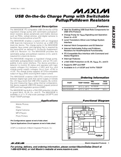
The MAX3353E is an I2C‑compatible USB On‑the‑Go (OTG) charge‑pump that provides VBUS power and signaling for dual‑role devices such as mobile phones, PDAs and digital cameras. It integrates switchable pull‑up/pull‑down resistors, a level‑shifter, ID detection, and a programmable VBUS power‑control block.
The device operates from a supply voltage of 2.6 V to 5.5 V, delivers a minimum 8 mA VBUS output current, and includes ±15 kV ESD protection on all USB pins. It is offered in a 5 × 4 mm UCSP package and a 16‑pin TSSOP package, and supports shutdown mode with quiescent current below 2 µA.
| Supply Voltage (VCC) | 2.6 V – 5.5 V |
|---|---|
| Logic Supply Voltage (VL) | 1.65 V – VCC |
| VBUS Output Current | 8 mA (minimum) |
| ESD Protection | ±15 kV |
| Package Types | 5 × 4 mm UCSP and 16‑pin TSSOP |
| Operating Temperature Range | -40 °C to +85 °C |
| Shutdown Quiescent Current | < 2 µA |
The device can source at least 8 mA of output current on VBUS.
It includes ±15 kV ESD protection on VBUS, ID_IN, D+, and D‑.
The supply voltage (VCC) range is 2.6 V to 5.5 V.
It is available in a 5 × 4 mm UCSP package and a 16‑pin TSSOP package.