
This datasheet provides a detailed description of the features and applications of the IDT72V2101/72V2111 3.3 V high density CMOS SuperSync FIFO™.
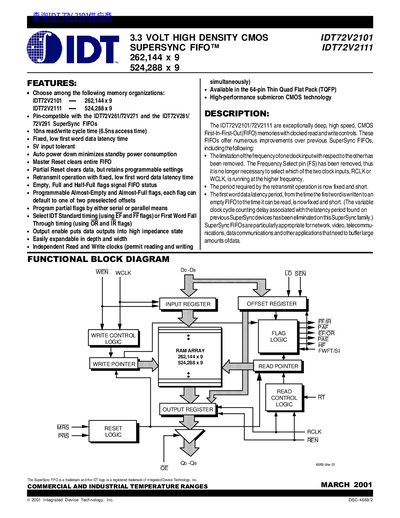
The IDT72V2101 and IDT72V2111 are 3.3 V high‑density CMOS SuperSync FIFO devices offering 262,144 × 9‑bit and 524,288 × 9‑bit depths. They feature a 10 ns read/write cycle, 5 V input tolerance, auto‑power‑down, and programmable flag thresholds.
The datasheet provides pin configurations, electrical characteristics (DC and AC), timing modes (IDT Standard and First Word Fall‑Through), and programming methods for flag offsets. Temperature ranges cover commercial (0 °C to +70 °C) and industrial (‑40 °C to +85 °C) environments.
| Depth (words) | 262,144 × 9 and 524,288 × 9 |
|---|---|
| Read/Write Cycle Time | 10 ns |
| Input Voltage Tolerance | 5 V input tolerant |
| Supply Voltage | 3.3 V |
| Standby Current | 20 mA |
During Master Reset the FWFT/SI pin selects either First Word Fall‑Through mode or IDT Standard mode.
The read/write cycle time is 10 ns.