
The IDT2309 is a 3.3V zero delay clock buffer designed for high-speed clock distribution applications within the range of 10 to 133MHz. It distributes one clock input to one bank of five outputs and one bank of four outputs, and each output bank has a separate output enable.
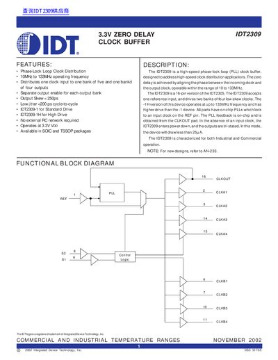
The IDT2309 zero‑delay clock buffer from Integrated Device Technology provides phase‑locked clock distribution for high‑speed designs. It features a built‑in PLL, separate output enable for each bank, and operates from a 3.3 V supply in both commercial and industrial temperature ranges.
Key specifications include a supply voltage range of –0.5 V to +4.6 V, operating frequency from 10 MHz to 133 MHz, output skew under 250 ps, cycle‑to‑cycle jitter ≤200 ps, and a power‑down current of 12 µA (commercial) or 25 µA (industrial). The device is offered in SOIC and TSSOP packages with standard and high‑drive versions.
| Supply Voltage Range (VDD) | –0.5 V to +4.6 V |
|---|---|
| Operating Frequency | 10 MHz to 133 MHz |
| Output Skew | < 250 ps |
| Input LOW Voltage Level (VIL) | 0.8 V |
| Output LOW Voltage (Standard Drive) | 0.4 V at 8 mA |
The device operates from 10 MHz up to 133 MHz.
Output skew is specified as less than 250 ps.
The VDD supply voltage range is –0.5 V to +4.6 V.