
This document describes the features and characteristics of IDT's CMOS SyncFIFO series products, including different storage organizations and read/write cycle time.
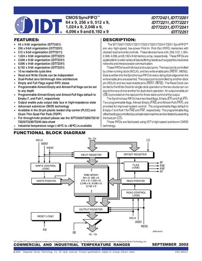
This document provides a comprehensive overview of the IDT SyncFIFO family of high‑speed, low‑power FIFO memories. It describes the various memory depths (64‑ to 8,192‑word configurations) and the 9‑bit data width, along with the functional block diagram and pin assignments for PLCC and TQFP packages.
Key features include dual‑clock operation, programmable almost‑empty and almost‑full flags, and support for both commercial (‑40 °C to +85 °C) and industrial temperature ranges. Electrical specifications such as supply voltage, leakage currents, and timing parameters are listed for each device variant.
| Memory organization | 64 × 9, 256 × 9, 512 × 9, 1,024 × 9, 2,048 × 9, 4,096 × 9, 8,192 × 9 |
|---|---|
| Clock cycle frequency | 40 MHz (minimum) |
| Supply voltage (Vee) | 5.0 V typical, 45 V min, 55 V max |
| Terminal voltage (VTERM) | -0.5 V to +7.0 V |
| Input leakage current | -1 µA min, 1 µA max |
Both commercial (‑40 °C to +85 °C) and industrial temperature ranges are available.
Almost‑Empty defaults to Empty+7 and Almost‑Full defaults to Full‑7.
WCLK is the Write Clock; data is written on each low‑to‑high transition when write enable pins are asserted.