
IDT5T9310 is a 2.5V LVDS 1:10 clock buffer from IDT
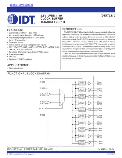
The IDT5T9310 is a 2.5 V LVDS 1:10 clock buffer designed for clock distribution in high‑speed systems. It offers guaranteed low skew (< 25 ps), very low duty‑cycle distortion (< 125 ps), and propagation delay under 1.75 ns, supporting up to 1 GHz operation. The device accepts a wide range of input standards (LVTTL, HSTL, eHSTL, LVEPECL, LVPECL, CML, LVDS) and provides ten selectable LVDS outputs, with hot‑insertable and over‑voltage tolerant inputs.
The datasheet details electrical characteristics, pin configuration, absolute maximum ratings, and recommended operating conditions. It specifies power‑supply voltage ranges, input and output voltage limits, and timing parameters such as skew and propagation delay. Ordering information and package details (VFQFPN) are also provided.
| Maximum Skew | < 25 ps |
|---|---|
| Duty‑Cycle Distortion | < 125 ps |
| Propagation Delay | < 1.75 ns |
| Maximum Operating Frequency | 1 GHz |
| Power‑Supply Voltage (VDD) | 0.5 V to 3.6 V |
| Operating Temperature Range | -40 °C to +85 °C |
| Package | VFQFPN |
| Number of LVDS Outputs | 10 |
The device guarantees a maximum skew of less than 25 ps.
It can operate up to 1 GHz.
It provides ten LVDS outputs.
Outputs should be disabled before entering power‑down mode.