
The AT49BV001A(N)(T) is a 2.7-volt-only in-system reprogrammable Flash Memory with features such as fast read access time, sector architecture, fast erase cycle time, and hardware data protection.
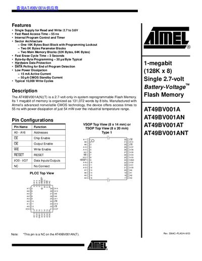
The AT49BV001A is a 1‑megabit, in‑system reprogrammable flash memory offered by Atmel. It operates from a single 2.7 V to 3.6 V supply and provides a fast 55 ns read access time. The device is organized into a 16 KB boot block, two 8 KB parameter blocks and two main memory blocks of 32 KB and 64 KB.
The datasheet describes the pin configurations for VSOP and TSOP packages, the command sequences for read, program, erase and lockout operations, and the electrical characteristics such as active current (15 mA), standby current (50 pA), and operating temperature ranges. It also details the boot block programming lockout feature and how it can be overridden with a 12 V reset pulse.
| Supply Voltage | 2.7 V to 3.6 V |
|---|---|
| Read Access Time | 55 ns |
| Active Current | 15 mA |
| Standby Current | 50 pA |
| Typical Write Cycles | ≥10 000 cycles |
| Memory Size | 1 Mbit (128 K × 8) |
| Boot Block Size | 16 KB |
| Parameter Block Size | 8 KB each (two blocks) |
| Main Memory Block Sizes | 32 KB and 64 KB |
| Operating Temperature (Case) | -40 °C to +85 °C |
| Temperature Under Bias | -55 °C to +125 °C |
The device operates from a single supply voltage between 2.7 V and 3.6 V.
It is rated for typical write and erase cycles of at least 10 000.
Apply a 12 V + 0.5 V signal to the RESET pin during the erase, sector erase, or byte programming operation.
The read access time is specified as 55 ns.