
This is a document about AT17F Series of In-System Programmable Configuration PROMs. This product is an easy-to-use, cost-effective configuration memory for Field Programmable Gate Arrays.
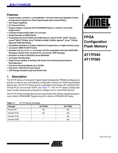
The AT17F040 and AT17F080 are In‑System Programmable configuration PROMs designed to store configuration programs for SRAM‑based FPGAs. They are offered in 8‑lead LAP, 20‑lead PLCC, 44‑lead PLCC and 44‑lead TQFP packages and support 2‑wire serial programming as well as cascade operation.
The manual covers device features, pin descriptions, block diagram, FPGA master serial mode, cascading of multiple configurators, and detailed programming procedures, including page‑paging and timing requirements.
| Operating voltage (output) | 3.3 V |
|---|---|
| I/O tolerance | 5 V tolerant |
| Endurance (typical) | 5,000 write cycles |
| Maximum serial download speed | 33 MHz |
| Low‑power standby mode | Supported |
The devices support serial download speeds up to 33 MHz.
Typical endurance is 5,000 write cycles.
The CE and RESET/OE pins control the tri‑state of the DATA output pin.
Cascading is done by connecting the CEO output of one device to the CE input of the next device in the chain.