
AS7C256A is a 5V 32K X 8 CMOS SRAM (Common I/O) chip produced by Alliance Semiconductor. It has the characteristics of high speed, low power consumption, and easy expansion.
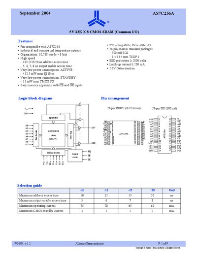
The AS7C256A is a high‑performance 5.0 V CMOS static RAM organized as 32,768 words × 8 bits. It offers address access times of 10‑20 ns and output‑enable times of 5‑8 ns, with active power consumption as low as 412.5 mW and standby power under 11 mW. The device is TTL‑compatible, features ESD protection, and is available in standard 28‑pin SOJ and TSOP packages.
Ordering information provides part numbers for commercial and industrial temperature ranges, with suffixes for lead‑free versions. The datasheet also includes timing diagrams, absolute maximum ratings, and recommended operating conditions for designers.
| Organization | 32,768 words × 8 bits |
|---|---|
| Address access time | 10‑20 ns |
| Output enable access time | 5‑8 ns |
| Active power consumption | ≤ 412.5 mW @ 10 ns |
| Standby power consumption | < 11 mW |
| Supply voltage | 4.5 V – 5.5 V |
| Operating temperature (commercial) | -40 °C – +125 °C |
| Operating temperature (industrial) | -40 °C – +85 °C |
The device operates from 4.5 V to 5.5 V.
Standby power consumption is less than 11 mW.
It is offered in 28‑pin SOJ, 28‑pin TSOP, and other JEDEC standard packages.
Address access time is 10‑20 ns and output‑enable access time is 5‑8 ns.