
ASM5I9773A is a low-voltage high-performance 200-MHz PLL-based zero delay buffer designed for high speed clock distribution applications. It features multiple output and input frequency ranges and supports 2.5V or 3.3V operation. The product also has features such as output enable/disable, low output duty cycle variation, and low output-output skew.
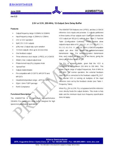
The ASM5I9773A zero‑delay buffer operates from a 2.5 V or 3.3 V supply and delivers up to twelve clock outputs across three banks. It features a PLL with bypass mode, spread‑spectrum support, and programmable output dividers that allow a wide range of output‑to‑input ratios.
The datasheet lists the device's electrical characteristics, including input and output voltage ranges, current consumption, and timing parameters, as well as absolute maximum ratings, package information (52‑pin 1.0 mm TQFP), and ordering codes for both tray and tape‑and‑reel formats.
| Operating voltage | 2.5 V or 3.3 V |
|---|---|
| Package | 52‑pin 1.0 mm TQFP |
| Output frequency range | 8.33 MHz to 200 MHz |
| Input frequency range | 6.25 MHz to 125 MHz |
| Maximum output duty‑cycle variation | 296 % (max) |
| Maximum output‑output skew | 300 ps (max) |
| Industrial temperature range | -40 °C to 185 °C |
| VCO frequency range | 200 MHz to 380 MHz |
The device operates from either a 2.5 V or a 3.3 V supply.
It is supplied in a 52‑pin 1.0 mm TQFP package.
The output frequency can be programmed up to 200 MHz.
It is rated for industrial temperatures from –40 °C to 185 °C.