
MAX2411A is a low-cost, low-power wireless radio front-end chip for TDD communication systems.
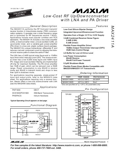
The MAX2411A is a RF front‑end transceiver that provides both up‑conversion and down‑conversion functions in a single, low‑cost package. It integrates a low‑noise amplifier (LNA), a variable‑gain power‑amplifier (PA) driver, and differential IF ports, enabling reduced component count for time‑division‑duplex (TDD) communication systems.
The document lists absolute maximum ratings, DC and AC electrical characteristics, pin descriptions, and typical operating curves such as gain, noise figure, power consumption, and impedance versus frequency. Key performance figures include a supply voltage range of 2.7 V–5.5 V, 60 mW receive power consumption, 2.4 dB LNA noise figure, and a 15 dB PA driver gain adjustable over a 35 dB range.
| Supply Voltage Range | 2.7 V to 5.5 V |
|---|---|
| Receive Power Consumption | 60 mW |
| Transmit Power Consumption | 90 mW |
| Shutdown Power Consumption | <0.3 µW |
| LNA Noise Figure | 2.4 dB (typical) |
| Mixer Noise Figure | 9.2 dB (typical) |
| PA Driver Gain | 15 dB (adjustable over 35 dB range) |
| Receive Mixer Conversion Gain | 9.4 dB (typical) |
The device operates from a single supply voltage of 2.7 V to 5.5 V.
In receive mode the MAX2411A consumes about 60 mW of power.
The LNA has a typical noise figure of 2.4 dB.
The receive mixer provides a typical conversion gain of 9.4 dB.