
The MAX19515 is a dual-channel analog-to-digital converter (ADC) with 10-bit resolution and a maximum sample rate of 65Msps. It accepts a wide 0.4V to 1.4V input common-mode voltage range, allowing DC-coupled inputs for a wide range of RF, IF, and baseband front-end components. The MAX19515 provides excellent dynamic performance from baseband to high input frequencies beyond 400MHz, making it ideal for zero-intermediate frequency (ZIF) and high-intermediate frequency (IF) sampling applications. The typical signal-to-noise ratio (SNR) performance is 60.1dBFS and typical spurious-free dynamic range (SFDR) is 82dBc at fIN = 70MHz and fCLK = 65MHz. The MAX19515 operates from a 1.8V supply. Additionally, an integrated, self-sensing voltage regulator allows operation from a 2.5V to 3.3V supply (AVDD). The digital output drivers operate on an independent supply voltage (OVDD) over the 1.8V to 3.5V range. The analog power consumption is only 43mW per channel at VAVDD = 1.8V. In addition to low operating power, the MAX19515 consumes only 1mW in power-down mode and 15mW in standby mode. Various adjustments and feature selections are available through programmable registers that are accessed through the 3-wire serial-port interface. Alternatively, the serial-port interface can be disabled, with the three pins available to select output mode, data format, and clock-divider mode. Data outputs are available through a dual parallel output.
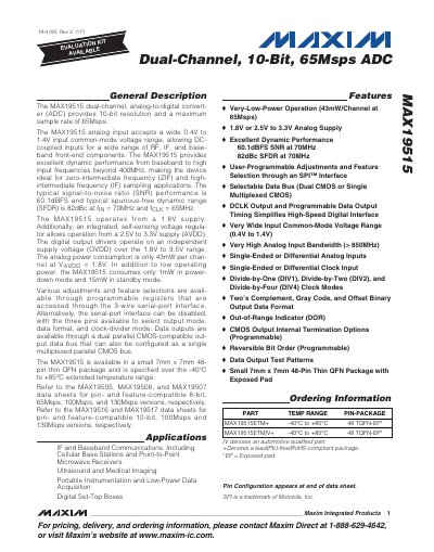
The MAX19515 dual‑channel analog‑to‑digital converter provides 10‑bit resolution and a maximum sample rate of 65 Msps. It accepts a wide 0.4 V to 1.4 V input common‑mode voltage range, supporting both DC‑coupled and AC‑coupled configurations for RF, IF and base‑band front‑end applications.
The device operates from a 1.8 V analog supply and includes an integrated self‑sensing regulator that allows operation from 2.5 V to 3.3 V. Power consumption is only 43 mW per channel at 65 Msps, with ultra‑low‑power modes down to 1 mW. It is offered in a 48‑pin thin QFN package (7 mm × 7 mm) and is specified for –40 °C to +85 °C operation.
| Maximum Sample Rate | 65 Msps |
|---|---|
| Input Common‑Mode Voltage Range | 0.4 V – 1.4 V |
| Power Consumption per Channel | 43 mW at 1.8 V |
| Typical SNR | 60.1 dBFS |
| Typical SFDR | 82 dBc |
| Package | 48‑pin thin QFN, 7 mm × 7 mm |
| Operating Temperature Range | ‑40 °C to +85 °C |
The MAX19515 can sample at up to 65 Msps.
Each channel consumes about 43 mW at a 1.8 V supply when running at 65 Msps.
The device is offered in a 48‑pin thin QFN package measuring 7 mm × 7 mm.