
The ALD2302A/ALD2302 are monolithic precision high performance dual voltage comparators built with advanced silicon gate CMOS tech- nology. The primary features are: very high typical input impedance of 1012Ω; low input bias current of 10pA; fast response time of 180ns; very low power dissipation of 175µA per comparator; and single (+5V) or dual (±5V) power supply operation. The input voltage range includes ground, which makes these compara- tors ideal for single supply low level signal detection with high source impedance. The outputs can source and sink current allowing for application flexibility. They can be used in either wired-OR connection without pull-up resistor or push-pull configuration. The ALD2302A/ ALD2302 can also be used in wired-OR connection with other open drain circuits such as the ALD2301/ALD2303 voltage comparators. The ALD2302A/ALD2302 voltage comparators are id
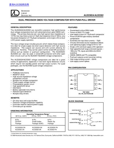
The ALD2302A/ALD2302 are monolithic dual voltage comparators built with advanced silicon‑gate CMOS technology. They feature very high input impedance, low input bias current (10 pA), fast response (180 ns), and low power dissipation (175 µA per comparator). The devices operate from a single (+5 V) or dual (+5 V) supply and support push‑pull output configurations.
Typical applications include PCMCIA instruments, MOSFET drivers, high‑source‑impedance voltage comparison circuits, LED drivers, oscillators, battery‑operated instruments, and relay drivers. The comparators provide on‑chip input and output buffers, eliminate the need for a second supply or pull‑up resistor, and can source/sink up to 60 mA per output.
| Input impedance | 10^12 Ω |
|---|---|
| Input bias current | 10 pA |
| Response time | 180 ns |
| Power dissipation | 175 µA per comparator |
| Supply voltage range | 4 V to 12 V |
| Output sinking current | 60 mA |
| Fanout | 30 LS TTL loads |
The typical input bias current is 10 pA.
The response time is typically 180 ns.
It can operate from 4 V up to 12 V.
Each output can sink up to 60 mA.