
This document provides technical information of APT6021, including main characteristics, maximum ratings, static electrical characteristics, etc.
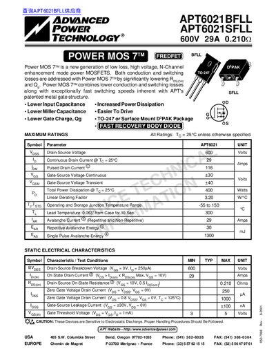
The APT6021BFLL and APT6021SFLL are members of the Power MOS 7™ family, offering low input and Miller capacitance, reduced gate charge, and fast switching speeds. They are packaged in TO‑247 or surface‑mount DPAK and feature a fast‑recovery body diode.
The document provides maximum ratings, static and dynamic electrical characteristics, diode ratings, and thermal data, including junction‑to‑case and junction‑to‑ambient thermal resistances. Package dimensions for TO‑247 and DPAK are also listed.
| Drain‑Source Voltage (VDS) | 600 V |
|---|---|
| Continuous Drain Current (ID) | 29 A |
| Pulsed Drain Current (ID(pulse)) | 116 A |
| Gate‑Source Voltage (continuous) | +30 V |
| Total Power Dissipation (PD) | 400 W |
| On‑State Resistance (RDS(on)) | 0.210 Ω |
| Input Capacitance (Ciss) | 3310 pF |
| Output Capacitance (Coss) | 590 pF |
| Total Gate Charge (Qg) | 76 nC |
| Turn‑on Delay Time (t(on)) | 15 ns |
| Rise Time (tr) | 10 ns |
| Junction‑to‑Case Thermal Resistance (RθJC) | 0.31 °C/W |
| Junction‑to‑Ambient Thermal Resistance (RθJA) | 40 °C/W |
The device is rated for a maximum drain‑source voltage of 600 V.
It can handle a continuous drain current of 29 A at a case temperature of 25 °C.
The gate threshold voltage is between 3 V and 5 V.
The on‑state resistance is 0.210 Ω.