
The document describes the features and characteristics of the Advanced Power P-CHANNEL ENHANCEMENT MODE Electronics Corp. POWER MOSFET, including simple drive requirement, voltage and current range, temperature characteristics, etc.
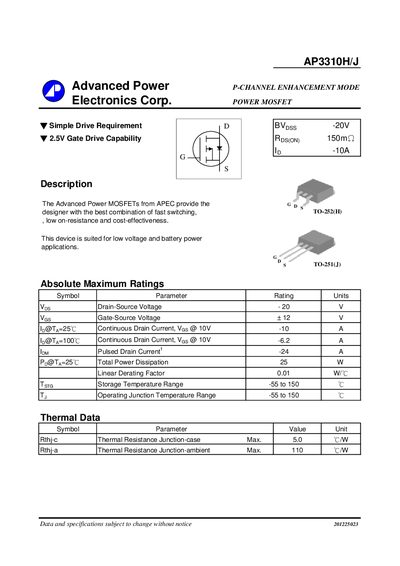
The AP3310H/J P‑channel MOSFET from Advanced Power is designed for low‑voltage and battery‑powered applications. It offers a drain‑source voltage rating of -20 V, gate‑source rating of +12 V, and continuous drain currents of -10 A at 25 °C and -6.2 A at 100 °C. The device features low on‑resistance and a total power dissipation capability of 25 W.
Key electrical characteristics include a pulsed drain current of -24 A, input capacitance of 300 pF, output capacitance of about 180 pF, and total gate charge of 6 nC. Thermal specifications list a junction‑to‑case resistance of 5.0 °C/W and junction‑to‑ambient resistance of 110 °C/W, supporting reliable operation across a wide temperature range.
| Drain‑Source Voltage (Vds) | -20 V |
|---|---|
| Gate‑Source Voltage (Vgs) | +12 V |
| Continuous Drain Current (25 °C) | -10 A |
| Continuous Drain Current (100 °C) | -6.2 A |
| Pulsed Drain Current | -24 A |
| Total Power Dissipation | 25 W |
| Thermal Resistance Junction‑Case | 5.0 °C/W |
| Thermal Resistance Junction‑Ambient | 110 °C/W |
| Input Capacitance (Ciss) | 300 pF |
| Output Capacitance (Coss) | 180 pF |
| Reverse Transfer Capacitance (Cres) | 60 pF |
| Total Gate Charge (Qg) | 6 nC |
| Turn‑on Delay Time | 25 ns |
The device is rated for a drain‑source voltage of -20 V.
It can handle a continuous drain current of -10 A at 25 °C.
The MOSFET can dissipate up to 25 W of power.
The input capacitance is specified as 300 pF.