
The L2720D is a low drop dual power operational amplifier with an output current of 1A. It operates at low voltages and can be used with single or split power supplies. The L2720D is suitable for a wide range of applications, such as servo amplifiers and power supplies. Its features include low input offset voltage, large common-mode and differential mode range, low saturation voltage, thermal shutdown, and clamp diode.
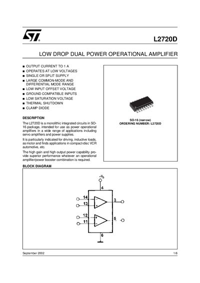
The L2720D is a monolithic low‑drop dual‑power operational amplifier offered in an SO‑16 package. It is intended for use in servo amplifiers, power supplies, and other applications that require high gain and high output power, such as driving inductive loads and motors.
The datasheet includes pin‑out diagrams, absolute maximum ratings, electrical characteristics (supply voltage, input offset, gain‑bandwidth, etc.), thermal data, mechanical dimensions, and safety notices. These details help designers evaluate the device for their circuits and ensure reliable operation within specified limits.
| Supply Voltage (Single) | 4 V to 28 V |
|---|---|
| Peak Supply Voltage (60 ms) | 50 V |
| Quiescent Drain Current | 10 mA to 15 mA |
| Input Offset Voltage | 10 mV |
| Gain‑Bandwidth Product | 1.2 MHz |
| Thermal Resistance (J‑A) | 95 °C/W |
The L2720D can tolerate a peak supply voltage of up to 50 V for 60 ms.
The typical gain‑bandwidth product is 1.2 MHz.
The input offset voltage is specified as 10 mV.
Thermal shutdown occurs at a junction temperature of 145 °C.