
The AT49BV/LV001(N)(T) is a 3-volt only in-system reprogrammable Flash Memory. Its 1 megabit of memory is organized as 131,072 words by 8 bits. Manufactured with Atmel’s advanced nonvolatile CMOS technology, the device offers access times to 70 ns with power dissipation of just 90 mW over the commercial temperature range. When the device is deselected, the CMOS standby current is less than 50 µA.
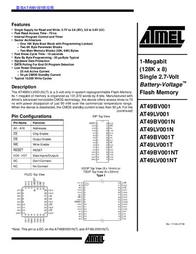
The AT49BV001/AT49LV001 family is a 1‑Megabit (128K × 8) in‑system reprogrammable flash memory offered in several package types (PDIP, PLCC, TSOP, VSOP). It operates from a single 3‑volt supply and features a fast 70 ns read access time, low power consumption, and up to 10,000 write/erase cycles.
The device includes a 16 KB boot block with optional programming lockout, two 8 KB parameter blocks, and two main memory blocks (32 KB and 64 KB). Programming is performed byte‑by‑byte with optional data‑polling or toggle‑bit detection, and the boot block can be protected or overridden via a 12 V reset pin.
| Supply Voltage (BV) | 2.7 V to 3.6 V |
|---|---|
| Read Access Time | 70 ns |
| Active Current | 25 mA |
| Standby Current (CMOS) | 50 pA |
| Typical Write Cycles | 10,000 |
| Memory Size | 1 Megabit (128 K × 8) |
| Boot Block Size | 16 KB |
| Parameter Block Size | 8 KB each (two blocks) |
| Main Memory Block Sizes | 32 KB and 64 KB |
The AT49BV001 operates from a single supply of 2.7 V to 3.6 V.
The device is rated for typical 10,000 write/erase cycles.
The boot block includes a programming lockout feature that, once enabled, prevents any further programming of that block.
Yes, applying a 12 V reset signal during erase or programming operations overrides the lockout.