
CDC5801 is a low jitter clock multiplier and divider with programmable delay and phase alignment. It features a single-ended input and a differential output, supporting LVPECL, LVDS and LVTTL signal levels. CDC5801 operates in the frequency range of 19 MHz to 125 MHz, with an output frequency range of 150 MHz to 500 MHz. It has a 2.6 mUI programmable bidirectional delay step, with a typical phase jitter of 8.0-ps (12 kHz to 20 MHz) @ 500 MHz and a typical RMS period jitter of 2.1-ps (entire frequency band) @ 500 MHz. CDC5801 supports three power operating modes to minimize power consumption. It has a typical power consumption of 200 mW@500 MHz. CDC5801 is packaged in a Shrink Small-Outline Package (DBQ), with no external components required for PLL. It also has a Spread Spectrum Clock Tracking ability to reduce EMI. CDC5801 is suitable for use in video graphics, gaming products, data communications and telecommunications.
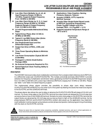
The CDC5801 device multiplies or divides a single‑ended reference clock (REFCLK) to produce differential output clocks (CLKOUT/CLKOUTB). It offers multiplication ratios of ×4, ×6, ×8 and division ratios of ÷2, ÷3, ÷4, with programmable bidirectional delay steps of 2.6 mUI and a phase‑aligner that can zero‑delay or offset the output relative to REFCLK.
The datasheet details electrical characteristics, absolute maximum ratings, recommended operating conditions, jitter performance, and mechanical dimensions of the DBQ plastic‑SO package. Typical power consumption is 200 mW at 500 MHz, and the device operates from –40 °C to 85 °C.
| Typical phase jitter | 8.0 ps (12 kHz‑20 MHz) |
|---|
Each rising edge on the DLYCTRL terminal advances or delays the output by a 2.6‑mUI step (1/384 of the output period).
At 500 MHz the accumulated phase jitter is about 8 ps (measured from 50 kHz to 80 MHz).