
This guide introduces the overclocking methods of the GIGABYTE A55 chipset motherboard, including CPU overclocking, memory overclocking, memory timing optimization, etc.
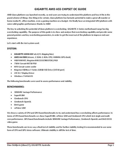
The document provides an overview of the AMD Llano platform and the Gigabyte A55M‑S2V motherboard, describing the overclocking potential of the CPU, GPU and memory. It outlines the test system, benchmarks used, and the methodology for adjusting the reference (BCLK) clock to increase overall performance.
Detailed sections cover key parameters such as BCLK limits, memory speed and timing adjustments, voltage settings for CPU, GPU and memory, and recommended BIOS and Windows power options. Final results show performance gains at 3.4 GHz and 3.7 GHz overclocks, with charts comparing benchmark scores before and after tuning.
| Maximum BCLK | 168 MHz |
|---|---|
| Maximum CPU frequency achieved | 3.7 GHz |
| Memory frequency at 3.4 GHz OC | 2287 MHz |
| Maximum memory voltage | 1.75 V |
| Maximum GPU voltage | 1.45 V |
The BIOS allows a maximum BCLK of 168 MHz.
The guide achieved a stable CPU frequency of 3.7 GHz, about 1 GHz above stock.
Memory modules can be run up to 1.75 V, with 1.65 V being typical.
Use Native IDE mode; AHCI may cause problems when BCLK exceeds 108 MHz.