
MDU28C is a dual channel HCMOS interfaced fixed delay line, which can achieve 10ns, 12ns, 16ns, 20ns and 25ns delay on two independent delay lines respectively
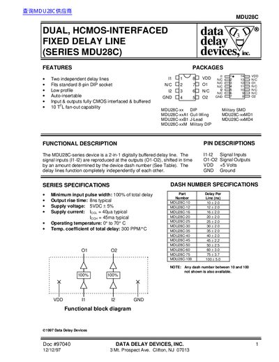
The MDU28C is a dual, HCMOS‑interfaced fixed delay line available in several package types, including standard 8‑pin DIP, gull‑wing, J‑lead and military variants. Each device provides two completely independent delay lines with fan‑out capability of 10 TTL loads. The delay amount is set by the dash number (e.g., MDU28C‑10, MDU28C‑20, etc.).
The device operates from a 5 VDC supply (±5%) and requires a 0.1 µF bypass capacitor close to the VDD pin for stable performance. Electrical characteristics include a typical output rise time of 8 ns, supply current of 40 µA, and operating temperature range of 0 °C to 70 °C. Detailed absolute maximum ratings and DC electrical characteristics are provided for design reference.
| Minimum input pulse width | 100% of total delay |
|---|---|
| Output rise time | 8 ns typical |
| Supply voltage | 5 VDC ±5% |
| Supply current | 40 µA typical |
| Operating temperature | 0 °C to 70 °C |
| Temp coefficient of total delay | 300 ppm/°C |
| High level output voltage | 3.98 V |
| Low level output voltage | 0.15 V |
| High level input voltage | 3.15 V |
| Low level input voltage | 1.35 V |
The MDU28C provides two independent delay lines.
The device requires a 5 VDC supply with a tolerance of ±5%.
A 0.1 µF capacitor from VDD to GND placed as close as possible to the VDD pin is recommended.
The typical output rise time is 8 ns.